local copy of blog by Ken Shirriff
Fixing the core memory in a vintage IBM 1401 mainframe
I recently had the chance to help fix one of the vintage IBM 1401 computer systems at the Computer History Museum when its core memory started acting up. As you might imagine, keeping old mainframes running is a difficult task. Most of the IBM 1401 restoration and repairs are done by a team of retired IBM engineers. But after I studied the 1401's core memory system in detail, they asked if I wanted to take a look at a puzzling memory problem: some addresses ending in 2, 4 or 6 had started failing.
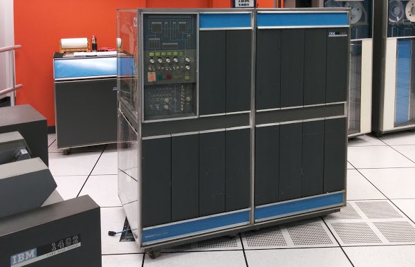
An IBM 1401 mainframe computer at the Computer History Museum. Behind it to the left is the IBM 1406 Storage Unit, providing an additional 12,000 characters of storage. IBM 729 tape drives are at the right and an IBM 1402 Card Read Punch is at the far left.
The IBM 1401 was low-end business computer that became the most popular computer of the early 1960s due to its low cost: $2500 a month, Like most computers of its era it uses ferrite core memory, which stores bits on tiny magnetized rings. The photo below shows a closeup of the ferrite cores, strung on red wires.
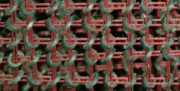
Closeup of the core memory in the IBM 1401 mainframe, showing the tiny ferrite cores.
The 1401 had only 4,000 characters of storage internally, but could hold 16,000 characters with the addition of the IBM 1406 Storage Unit. This core memory expansion unit was about the size of a dishwasher and was connected to the 1401 computer by two thick cables.[1] This 12,000 character expansion box could be leased for $1575 a month or purchased for $55,100. (In comparison, a new house in San Francisco was about $27,000 at the time.) The failing memory locations were all in the same 4K block in the IBM 1406, which helped narrow down the problem.
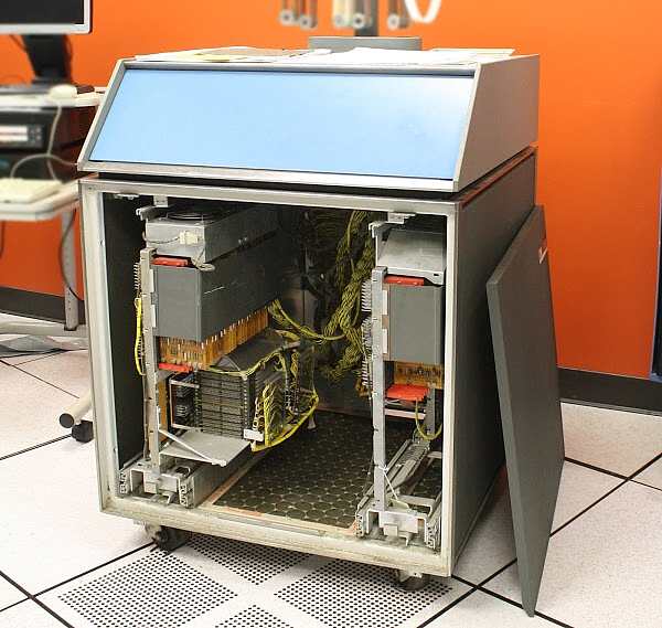
A view inside the IBM 1406 Storage Unit, which provides 12,000 characters of storage for the IBM 1401 mainframe. At the left is the 8,000 character core module below the cards that control it. The 1406 contains two separate core memory modules: one with 8,000 characters and one with 4,000 characters. In the picture above, the 8K core module is visible on the left, while the 4K core module is out of sight at the back right. Associated with each core module is circuitry to decode addresses, drive the core module, and amplify signals from the module; these circuits are in three rows of cards above each module. The 1406 also provided an additional machine opcode (Modify Address) for handling extended addresses. Surprisingly, the logic for this new opcode is implemented in the external 1406 box (the cards on the right), not in the 1401 computer itself. The 1406 box also contains hardware to dump the entire contents of memory to the line printer, performing a core dump.
The circuits in the 1406 (and the 1401) are made up of Standardized Module System (SMS) cards. A typical card has a few transistors and implements a logic gate or two. Unlike modern transistors, these transistors are made from germanium, not silicon. The photo below shows rows of SMS cards inside the 1406. Note the metal heat sinks on the high-current transistors driving the core module.
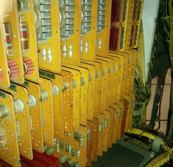
A closeup of SMS cards inside an IBM 1406 Storage Unit. The top cards have heat sinks on high-current driver transistors. The core memory is made from planes of 4,000 cores, as seen below. Each plane is built from a grid of 50 by 80 wires, with cores where the wires cross. By simultaneously energizing one of the 50 horizontal (X) wires and one of the 80 vertical (Y) wires, the core at the intersection of the two wires is selected. Each plane holds one bit of each character, so 8 planes are stacked to hold a full character.
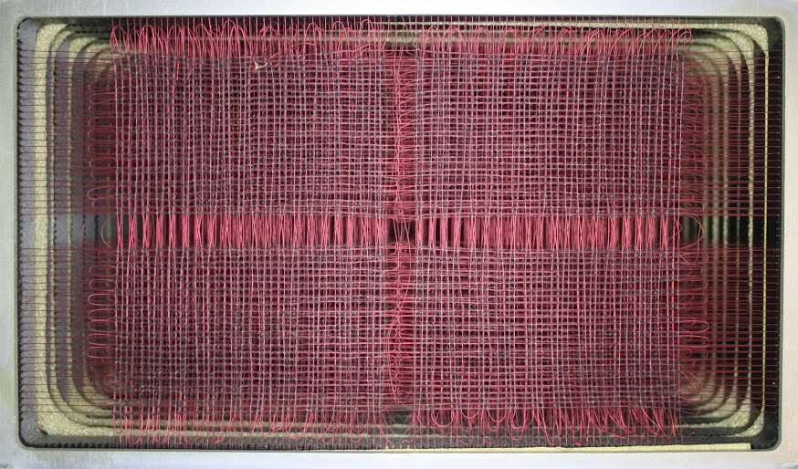
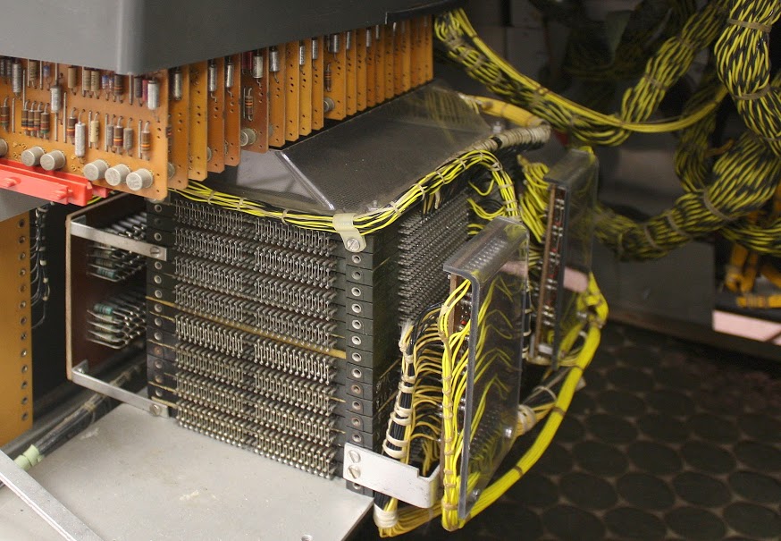
Core memory in the IBM 1401 mainframe. Each layer (plane) has 4,000 tiny cores in an 80x50 grid. Multiple planes are stacked to form the memory. The photo below shows the 8K memory module inside the 1406, built from a stack of 16 core planes. (Since a stack of 8 planes makes 4K, 16 planes make 8K.) Mounted on the right of the core module are the "matrix switches", which drive the X and Y select lines; my previous core memory article explains them.
The IBM 1401 predates 8-bit bytes, and it used 6-bit characters. Each character consisted of a 4-bit BCD (binary-coded decimal) digit along with two extra "zone" bits. By setting zone bits, letters and a few symbols could be stored. For instance, with both zone bits set, the BCD digit values 1 through 9 corresponded to the characters "A" through "I". Other zone bit combinations provided the rest of the alphabet. While this encoding may seem strange, it maps directly onto IBM punched cards, which have 10 rows for the digit and two rows for zone punches. This encoding was called BCDIC (Binary-Coded Decimal Interchange Code), and later became the much-derided EBCDIC (Extended BCDIC) encoding. (You may have noticed that 8 planes are used for 6-bit characters. One extra plane holds special "word mark" bits, and the other holds parity.)
The point of this digression into IBM character encoding is that a three-digit address also included 6 zone bits. Four of these bits were used as part of the address, allowing 16,000 addresses in total.[2] For example, the address 14,578 would be represented as the digits 578 along with the appropriate zone bits, so the resulting address would be represented as the three characters "N7H".[3]
Getting back to the problem with the memory unit, the 4K bank was failing with addresses ending in 2, 4 and 6. Looking at 2, 4 and 6, I immediately concluded that what these all had in common was the 2 bit was set. Except 4 doesn't have the 2 bit set. So maybe the problem was with even addresses. Except 0 and 8 worked. After staring at bit patterns a while, I became puzzled because 2, 4 and 6 didn't really have anything in common.
Looking at the logic diagrams reveals the hardware optimization that makes 2, 4, and 6 have something in common. Since the problem happened with specific unit digits, the problem was most likely in the address decoding circuitry that translates the unit digit to a particular select line.[4] The normal way of decoding a digit is to look at the 4 bits of the digit to determine the value. Unexpectedly, the decoder only looks at 3 bits; this reduces the hardware required, saving money. For instance, the digit 2 is detected below if the 4 bit is clear, the 1 bit is clear, and the 8 bit is clear. The digit 4 is detected if the parity (CD) bit is clear, the 4 bit is set, and the 1 bit is clear. The digit 6 is detected if the 1 bit is clear, the 2 bit is set, and the 4 bit is set.[5] Looking at the decode logic, decoding of the digits 2, 4, and 6 (and only these digits) tests that the 1 bit is clear. Now the failure starts to make sense. If something is wrong with the units 1-bit-clear signal, these digits would not be decoded properly and memory would fail in the way observed.
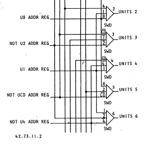
Every connection and circuit of the IBM 1401 is documented in an Automated Logic Diagram (ALD). These diagrams were generated by computer and put in a set of binders for use by service engineers. The code number 42.73.11.2 on the previous diagram provides the page number of the related ALD. While these diagrams are extremely detailed, they are nearly incomprehensible. Since I'm using copies of reduced 50-year-old line printer output, the ALDs are also barely readable.
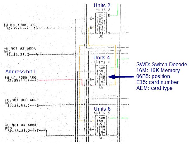
Now we can see the root cause of the problem. The unit address bit 1 (highlighted in red on the ALD) goes into pin A of the Units 4 card and is inverted. The inverted value (pin D, yellow) then goes to the Units 2 and Units 6 cards, generating the decode outputs (green). If something is wrong with this signal, addresses 2, 4, and 6 won't decode, which is exactly the problem encountered. Thus, the Units 4 card seemed like the problem.
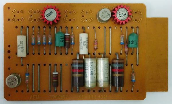
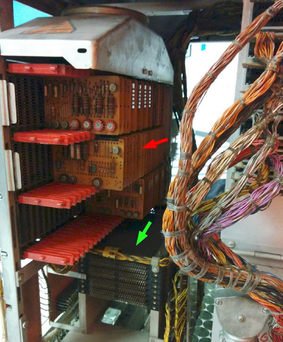
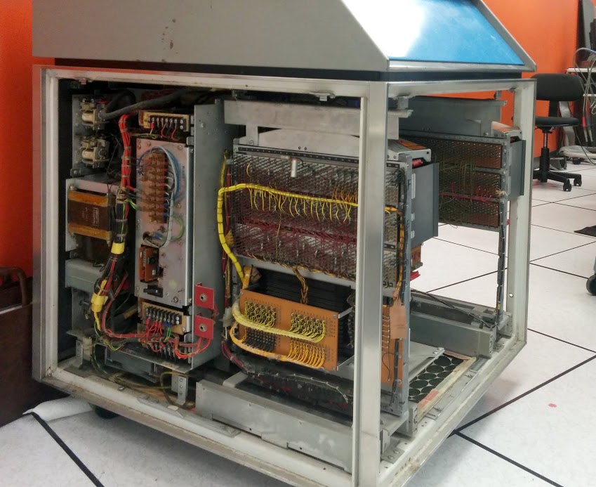
One convenient thing about the IBM 1401 and its peripherals is they are designed for easy maintenance. In many cases, you don't even need any tools. To get inside the IBM 1406, you just pop the front or side panels off (as shown below). The SMS cards have a metal cover to guide the cooling airflow, but that just pops off too. It's easy to attach an oscilloscope to see what's happening, although I didn't need to do that. The SMS cards themselves are easily pulled from their sockets. I'm told you don't even need to power down the system to replace cards, but of course I turned off the power.
I pulled out the card in slot E15, plugged in a replacement card from the 1401 lab's collection, and powered up the system. Much to my surprise, the memory worked perfectly after replacing the card. Some of the engineers (Stan, Marc, and Dave) tested the transistors on the bad card but didn't find any problems. After cleaning the bad card and swapping it back, the memory still worked, so there must have been some dirt or corrosion making a bad connection. They say this is the first problem they've seen due to bad connections, so the thick gold plating on the SMS card contacts must work well.
Conclusion
It's not every day one gets the chance to help fix a 50 year old mainframe, so it was an interesting experience. I was lucky that this problem turned out to be easy to resolve. The guys repairing the tape drives and card reader have much harder problems, since those devices are full of mechanical parts that haven't aged well.Thanks to the members of the 1401 restoration team and the Computer History Museum for their assistance. Special thanks to Stan Paddock, Marc Verdiell and Dave Lion for inviting me to investigate this problem.
The IBM 1401 is demonstrated at the Computer History Museum on Wednesdays and Saturdays (unless there is a hardware problem) so check it out if you're in Silicon Valley (schedule).
Notes and references
[1] The 1406 expansion unit was 29" wide, 30 5/8" deep and 39 5/8" high and weighed 350 lbs. The 10 foot cables between the 1401 computer and the 1406 storage unit are each 1 1/4" thick; one provides power and the other has signals. The 1406 generates 250 watts of heat, which is less than I would have expected. Details are in the installation manual.[2] The three-digit address has six zone bits in total. Four are used as part of the address. The other two zone bits to indicate an indexed address using one of three index registers (which are actually part of core, not separate registers). Indexed addressing was part of the "Advanced Programming" option which cost an extra $105 per month.
[3] For full information on converting addresses to characters, see the IBM 1401 Pocket Reference Manual, page 3.
[4] Scans of the Instructional Logic Diagrams (ILDs) are available online. The memory decode circuits are on page 56. Scans of the Automated Logic Diagrams (ALDs) are also available online; the core memory is in section 42.
[5] The IBM 1401 predates standardized logic symbols, so the logic diagram symbols may be confusing: the triangular symbol is an AND gate. The SWD (Switch Decode) card inverts its inputs, but that isn't shown on the logic diagram.
There are few subtleties in the decoding logic. You might think that the circuit described would decode a 0 digit as a 2 digit since the 1, 4, and 8 bits are clear. However, the IBM 1401 stores the digit 0 as the value 10 (8 bit and 2 bit set), since a blank is stored with all bits clear.
For the decoding using the parity bit, note that the IBM 1401 uses odd parity. For instance, the digit 4 (binary 0100) already has odd parity, so the CD (check digit) parity bit is clear. The digit 5 (binary 0101) has the CD parity bit set so three bits are set in total.
[6] The original idea of SMS cards was to build computers from a small set of standardized cards, but as you can guess from the complexity of the AEM card, engineers created highly-specialized SMS cards for specific purposes. IBM ended up with thousands of different SMS card types, defeating the advantages of standardization. I've created an SMS card database that describes a thousand different SMS cards.
[7] The 06B5 designation indicates which gate holds the card. (Each rack of cards is called a "gate" in IBM terminology. Confusingly, this has nothing to do with a logic gate.) The 06 indicates the 1406 frame. The B indicates a lower frame. Position 5 is in the back right. The same numbering system is used in the IBM 1401 itself. The 1401 is built around the same frame structure as the 1406, except with four frames, stacked 2x2. The left frames are numbered 01, and the right frames are 02. The frames on top are A, and the frames on the bottom are B. Gates 1 through 4 are in the front, and 5 through 8 continue around the back. A typical 1401 gate identifier is "01B2", which indicates the rack on the front of the 1401 below the console. (The use of frames to build computers and peripherals led to the term "main frame" to describe the processing unit itself.)